
Introduction
Huawei has previously released a series of car chargers with power ratings of 25W, 66W, and 88W, as well as an 80W wireless car charger, covering both wired and wireless charging needs to fully meet in-car charging demands.
Recently, a new member has joined the car charger family—the P0019. This new car charger maintains the same appearance, size, and port configuration as its predecessor, but brings a comprehensive upgrade in charging power. Supporting 100W fast charging across SCP, UFCS, PD3.0, and PPS protocols, it delivers excellent performance and compatibility with no compromises.
Not only does it support Huawei SuperCharge, but it’s also widely compatible with devices running iOS, HarmonyOS, Android, and more. It can fast-charge smartphones, laptops, tablets, smartwatches, earphones, gaming consoles, and various other devices from different brands. Next, let’s take it apart to see its internal components and structure.
Product Appearance
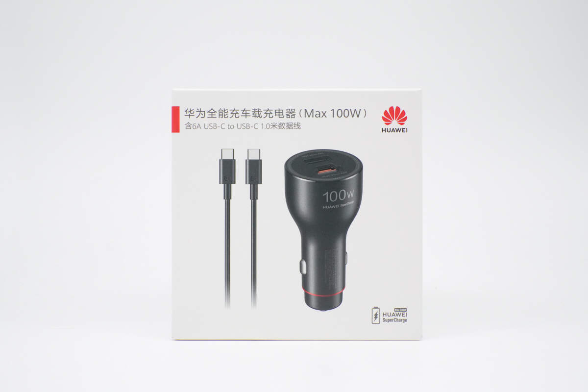
Huawei, product name, and appearance are printed on the front of the box.
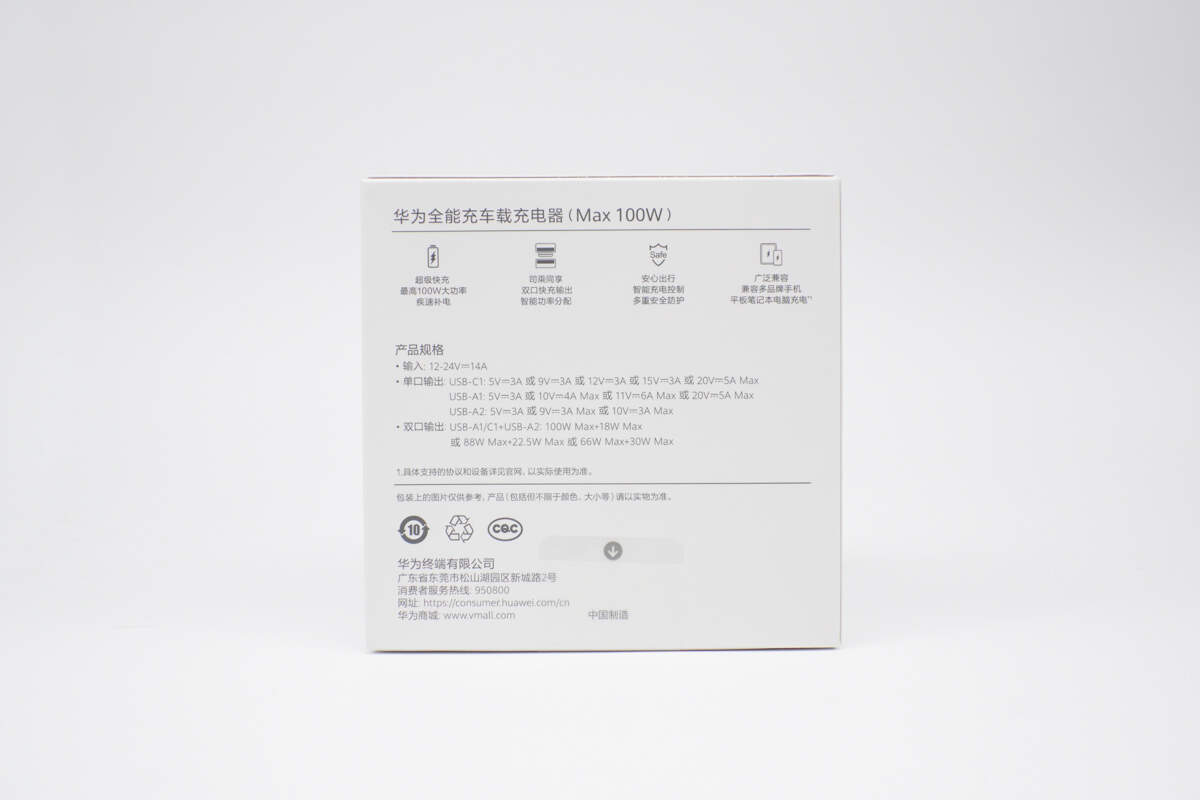
The back is printed with selling points and spec info.
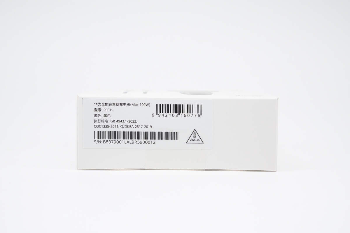
The sticker on the side displays information such as the product name, model, and color scheme.
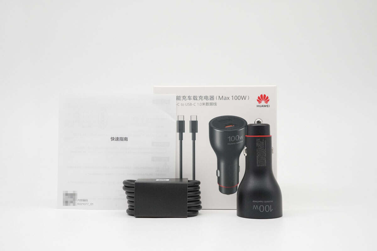
The package includes the car charger, cable, and more.
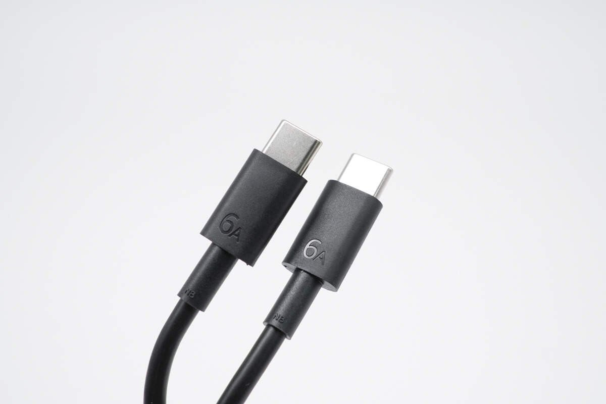
The connectors are engraved with "6A".
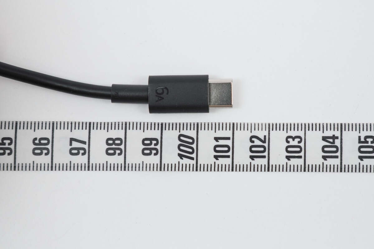
The length of the cable is about 1 m (3' 3.37'').
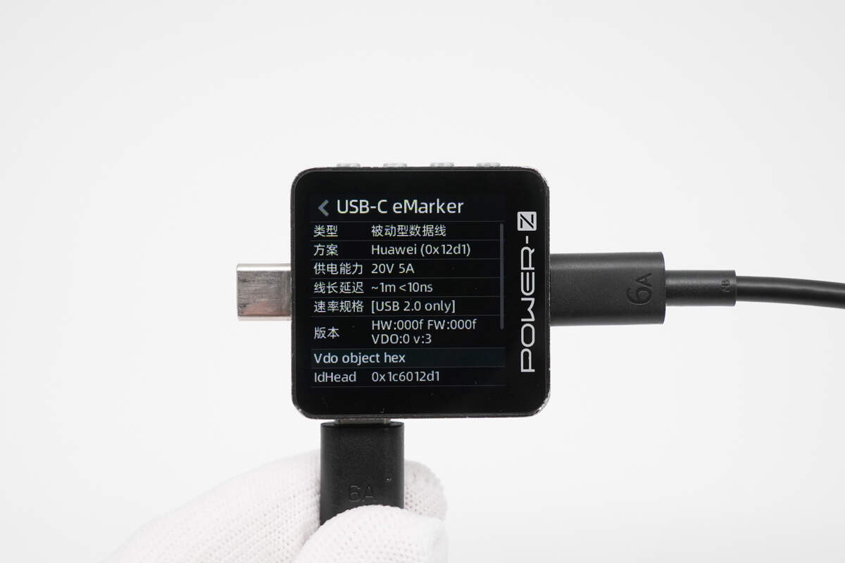
ChargerLAB POWER-Z KM003C shows that it has an E-Marker chip and supports power delivery of 20V 5A, enabling 100W PD fast charging.
It features a flame-retardant PC casing with a matte finish.
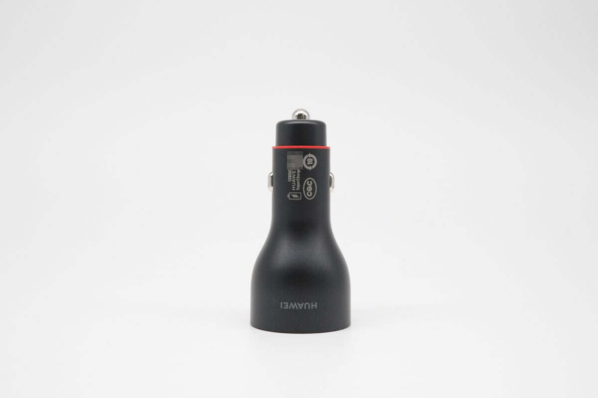
This side is printed with the HUAWEI logo and the CQC certification mark, among others.
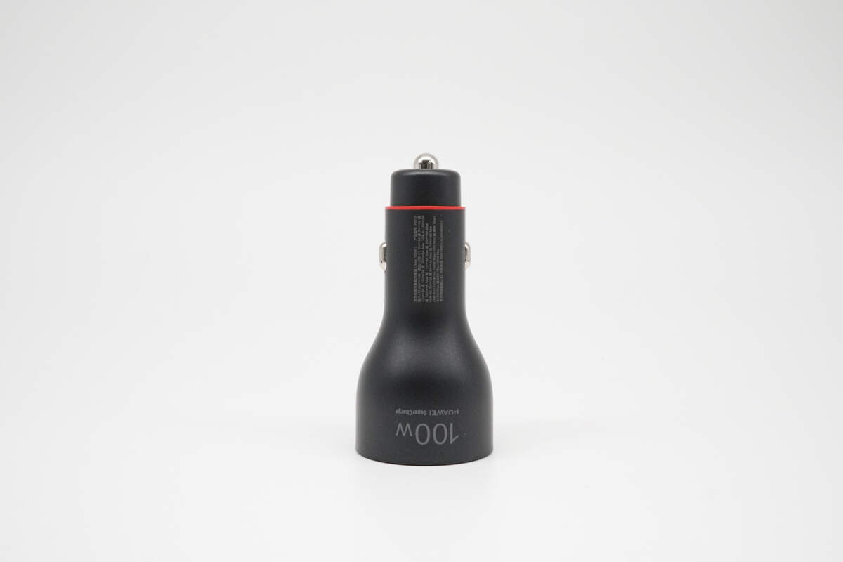
This side is printed with "100W HUAWEI SuperCharge" along with specification information.
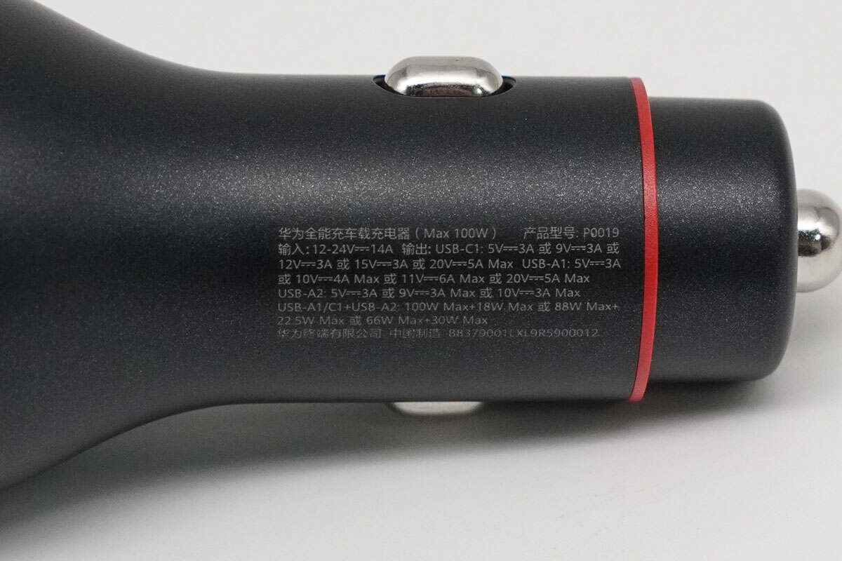
Model: P0019
Input: 12–24V 14A
Output:
USB-C1: 5V 3A, 9V 3A, 12V 3A, 15V 3A, 20V 5A Max
USB-A1: 5V 3A, 10V 4A Max, 11V 6A Max, 20V 5A Max
USB-A2: 5V 3A, 9V 3A Max, 10V 3A Max
USB-A1/C1 + USB-A2: 100W Max + 18W Max or 88W Max + 22.5W Max or 66W Max + 30W Max
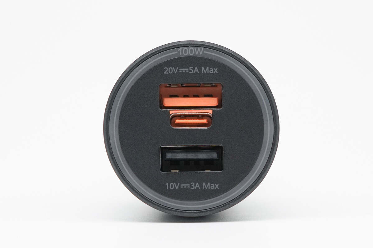
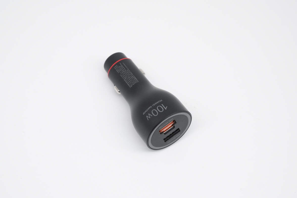
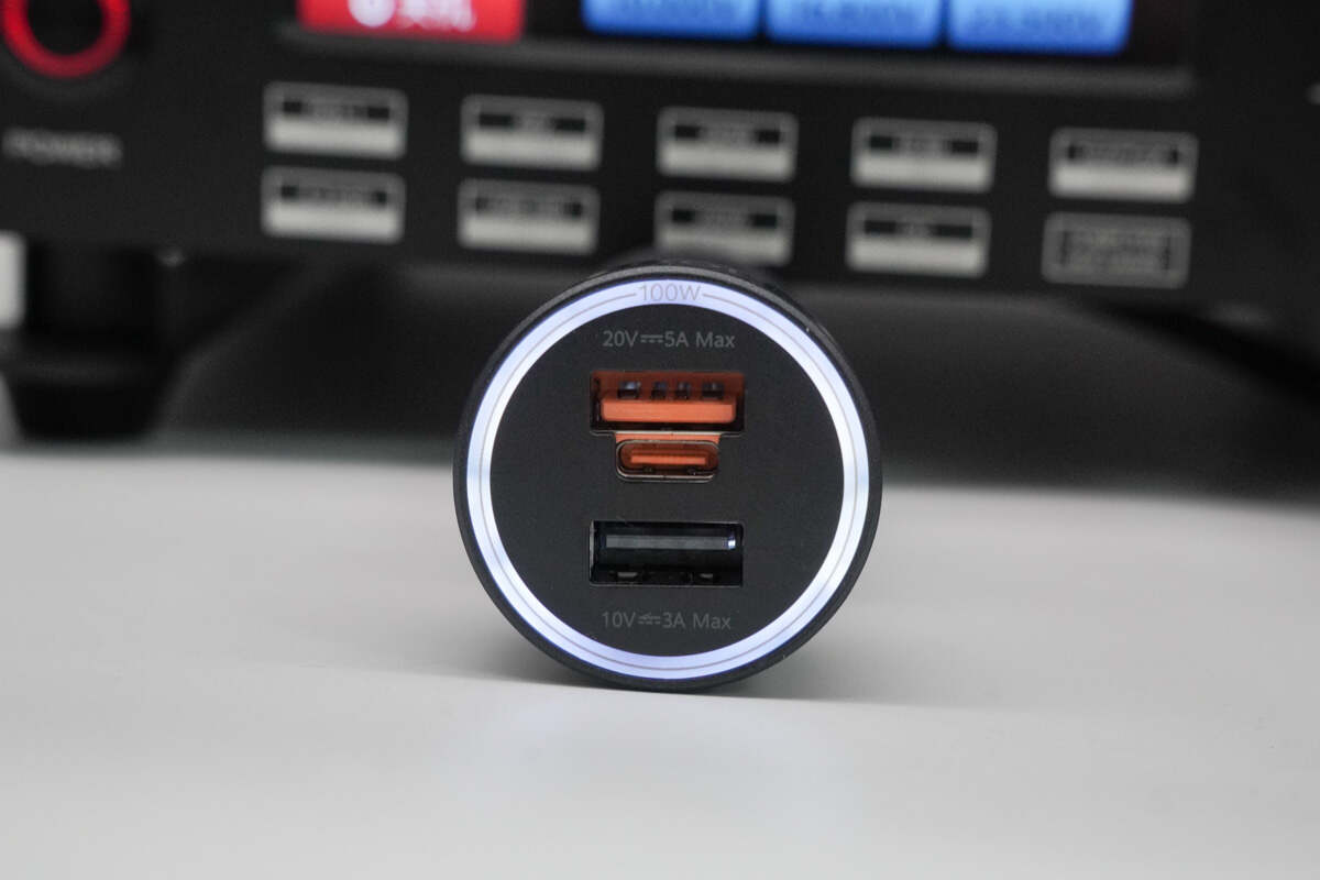
The top features a combined USB-A/USB-C port and a USB-A2 port, with a light ring around the edge.
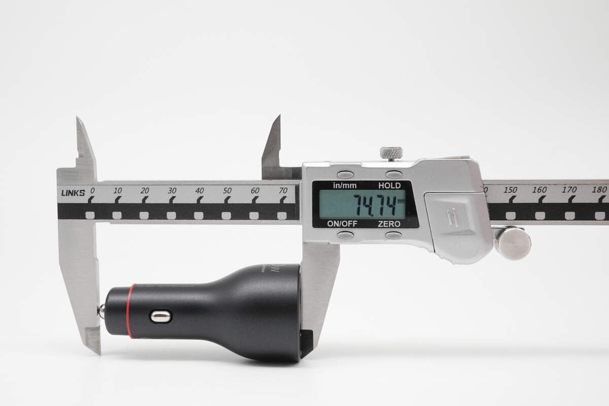
The length of the charger is about 74.74 mm (2.94 inches).
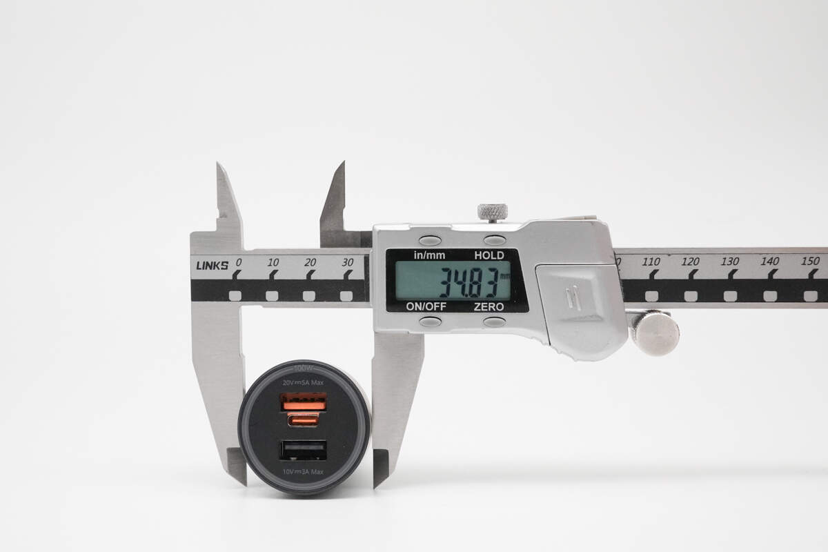
The diameter of the top is 34.83 mm (1.37 inches).
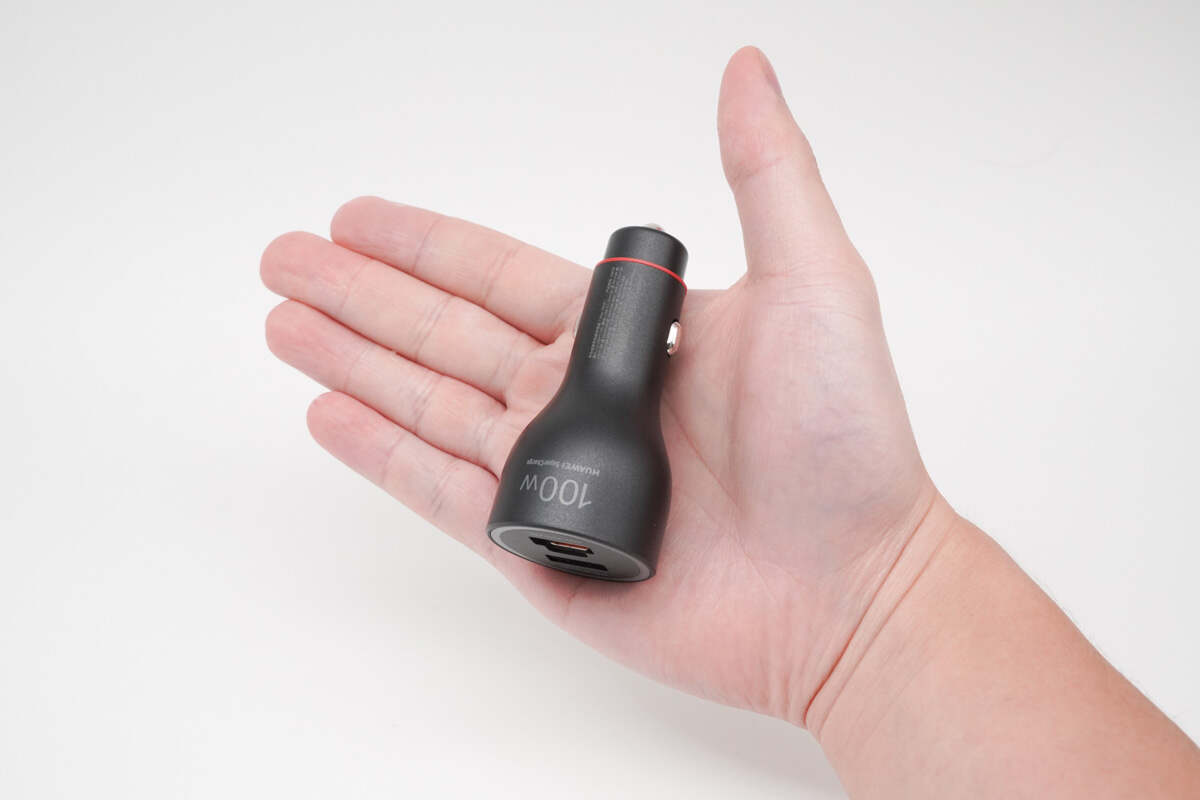
That's how big it is in the hand.
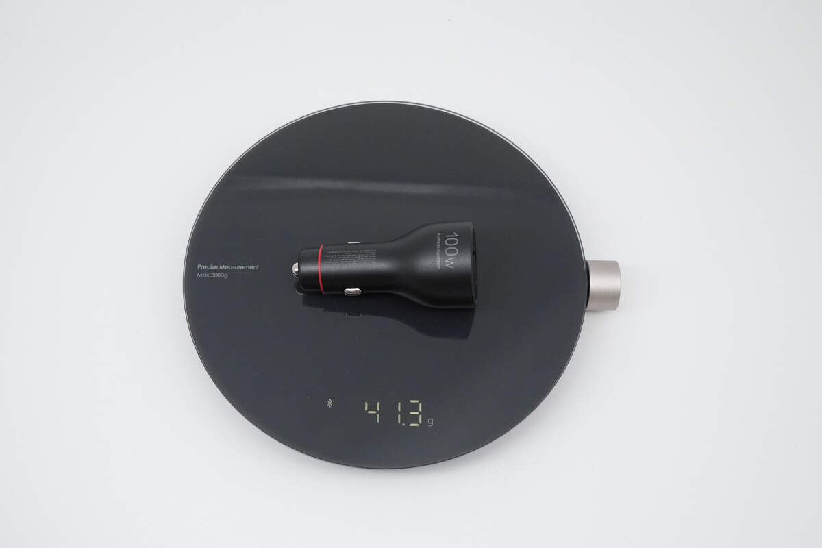
The weight is about 41 g (1.45 oz).
When powered on, the light ring illuminates white.
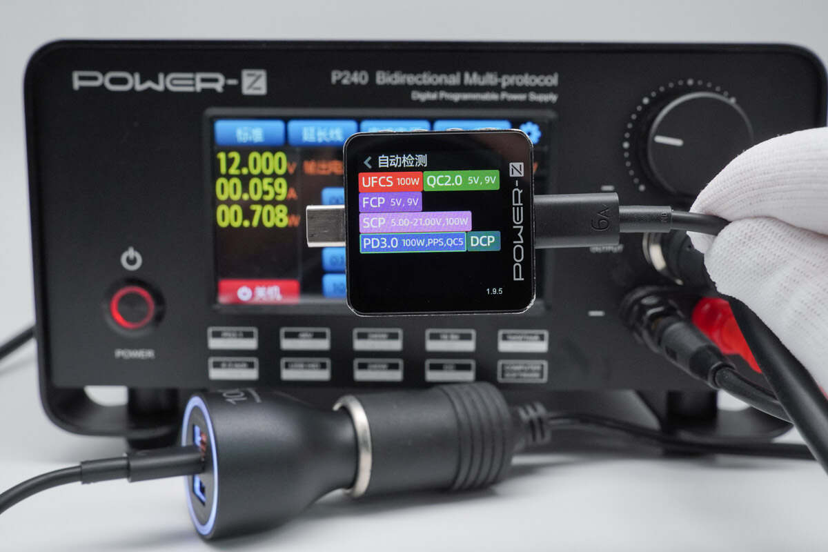
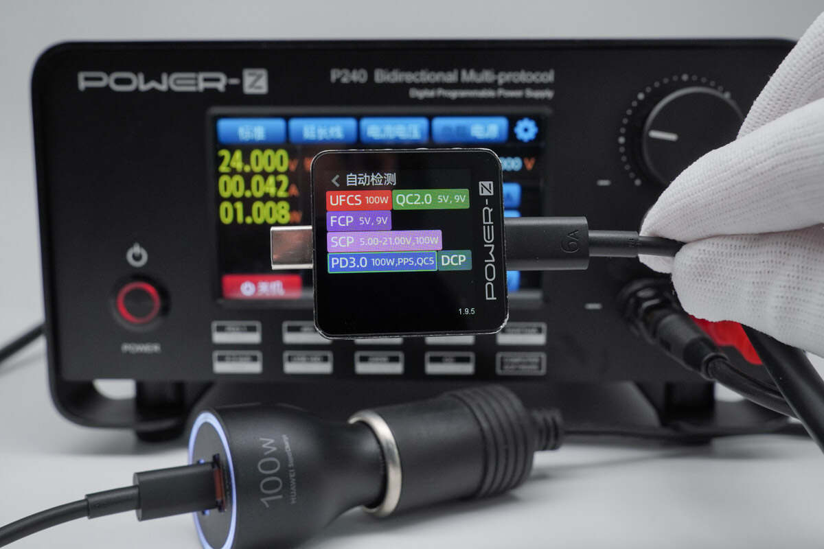
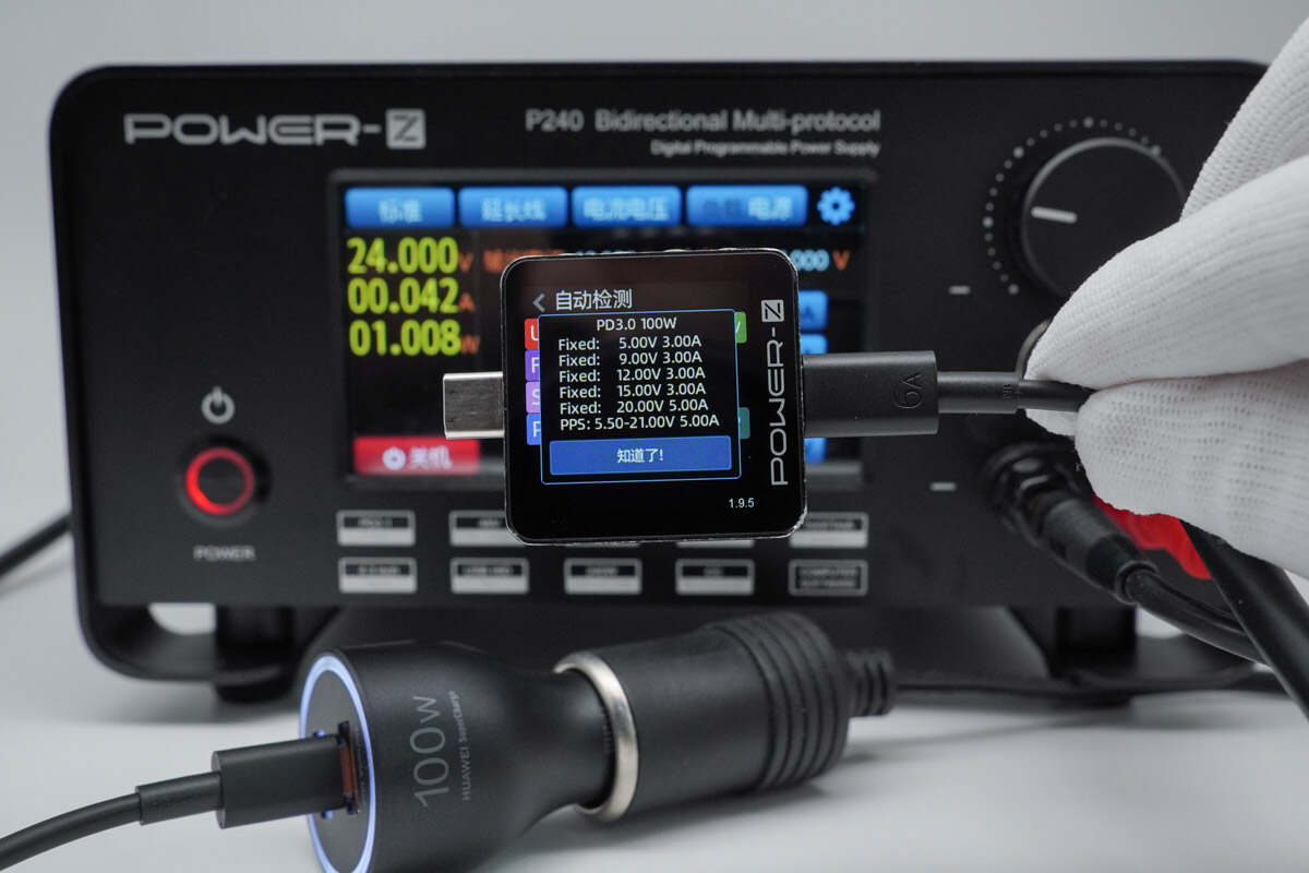
Simulating a 12V DC input, the USB-C1 port was found to support UFCS, QC2.0/5, FCP, SCP, PD3.0, PPS, and DCP charging protocols.
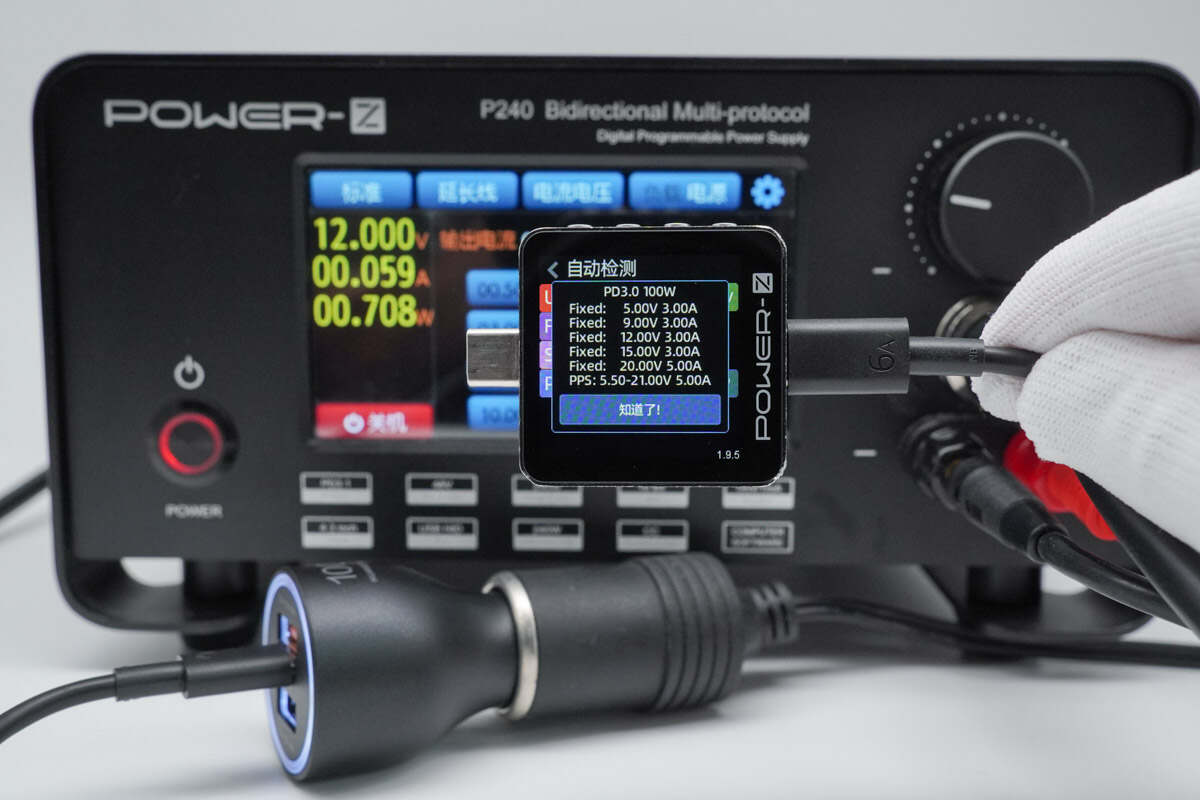
And it has five fixed PDOs of 5V3A, 9V3A, 12V3A, 15V3A, and 20V5A. It also has a set of PPS, which is 5.5-21V 5A.
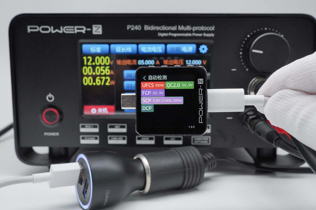
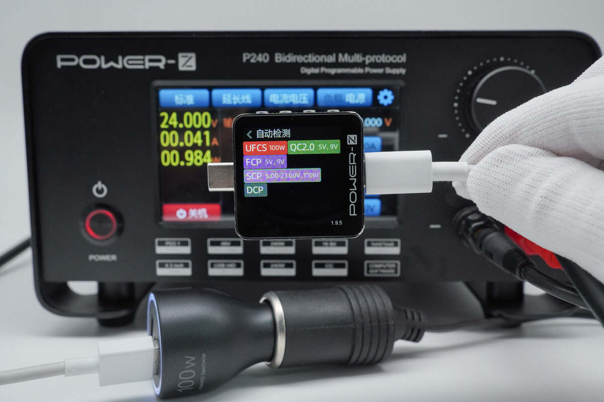
The USB-A1 port was found to support UFCS, QC2.0, FCP, SCP, and DCP charging protocols.
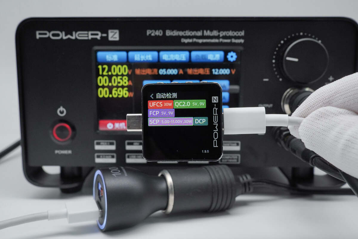
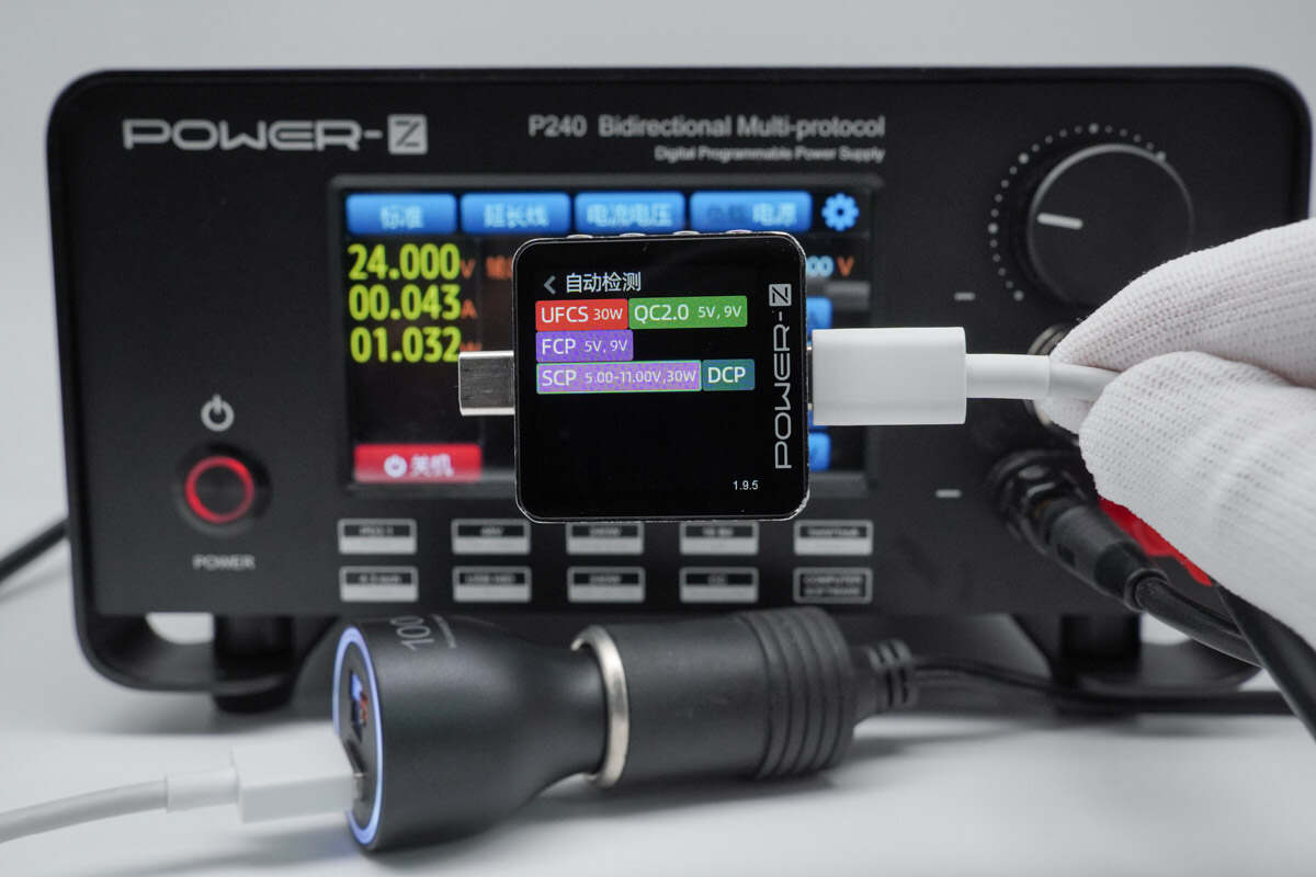
The USB-A2 port was found to support UFCS, QC2.0, FCP, SCP, and DCP charging protocols.
When simulating a 24V DC input, the USB-C1 port was found to support the same charging protocols as with a 12V DC input.
Additionally, the PDO messages are also the same.
The USB-A1 port was also found to support the same charging protocols as the 12V DC input.
The USB-A2 port was also found to support the same charging protocols as the 12V DC input.
Teardown
Next, let's take it apart to see its internal components and structure.
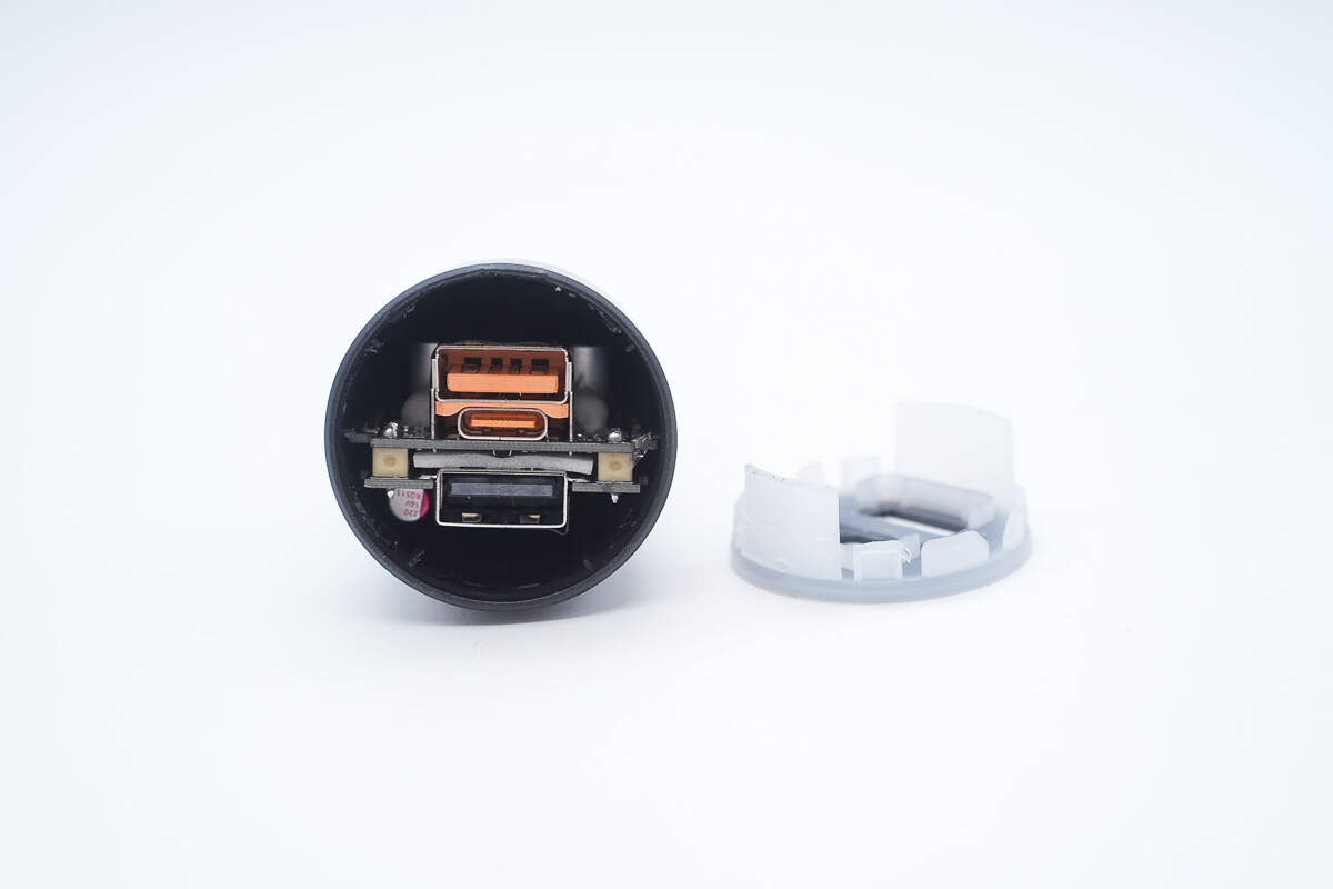
Remove the top casing, which is secured by snap-fit clips.
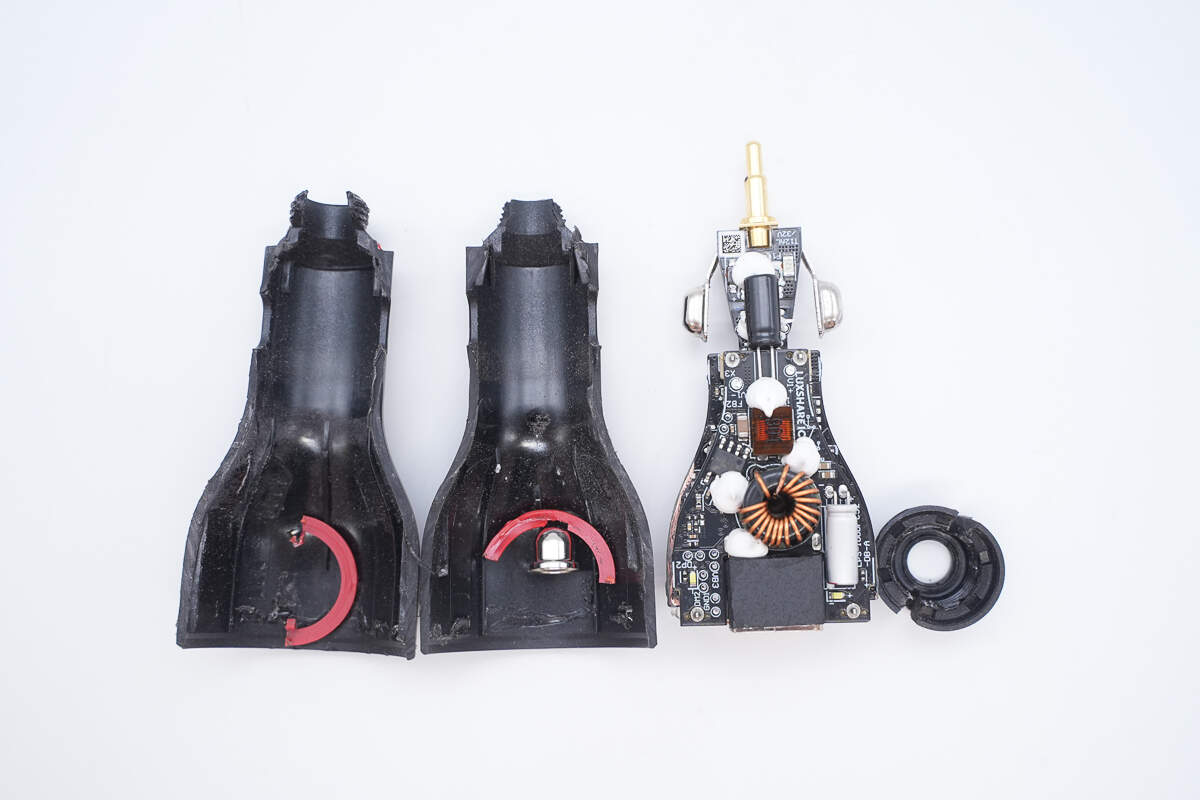
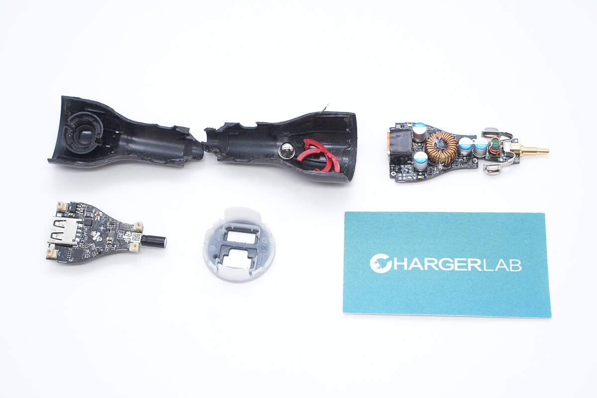
Cut the shell and take out the PCBA module.
The PCBA module uses a double-layer design, with components such as capacitors and inductors reinforced with adhesive.
Components such as capacitors and inductors on the other PCB are also reinforced with adhesive, and both USB-A sockets are insulated.
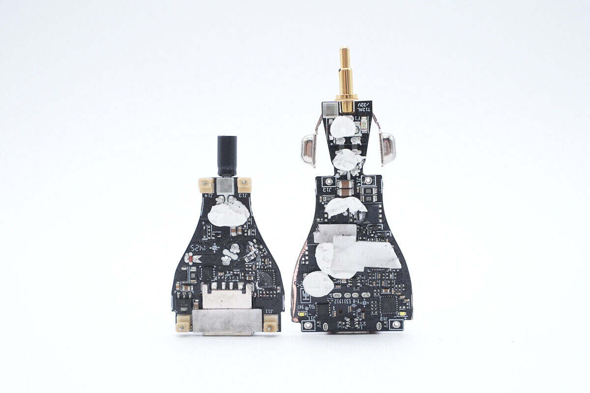
Separate the two PCBs, with a thermal pad between them to help dissipate heat.
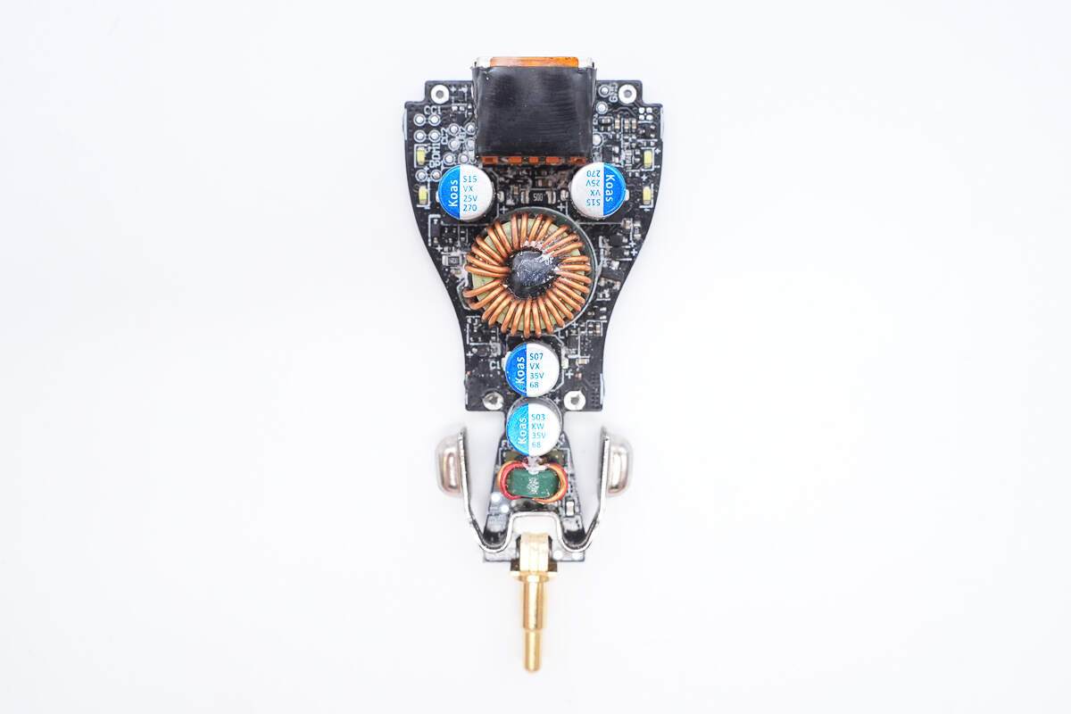
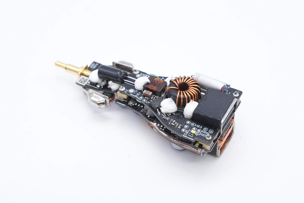
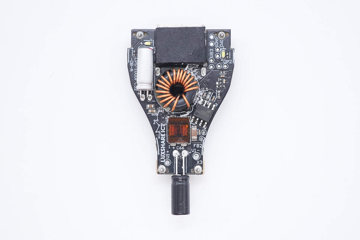
The front side of the PCB with the combined port is equipped with components such as a filter inductor, filter capacitor, and buck-boost inductor.
On the back are a synchronous buck-boost controller, a buck-boost MOSFET, a protocol chip, and a VBUS MOSFET.
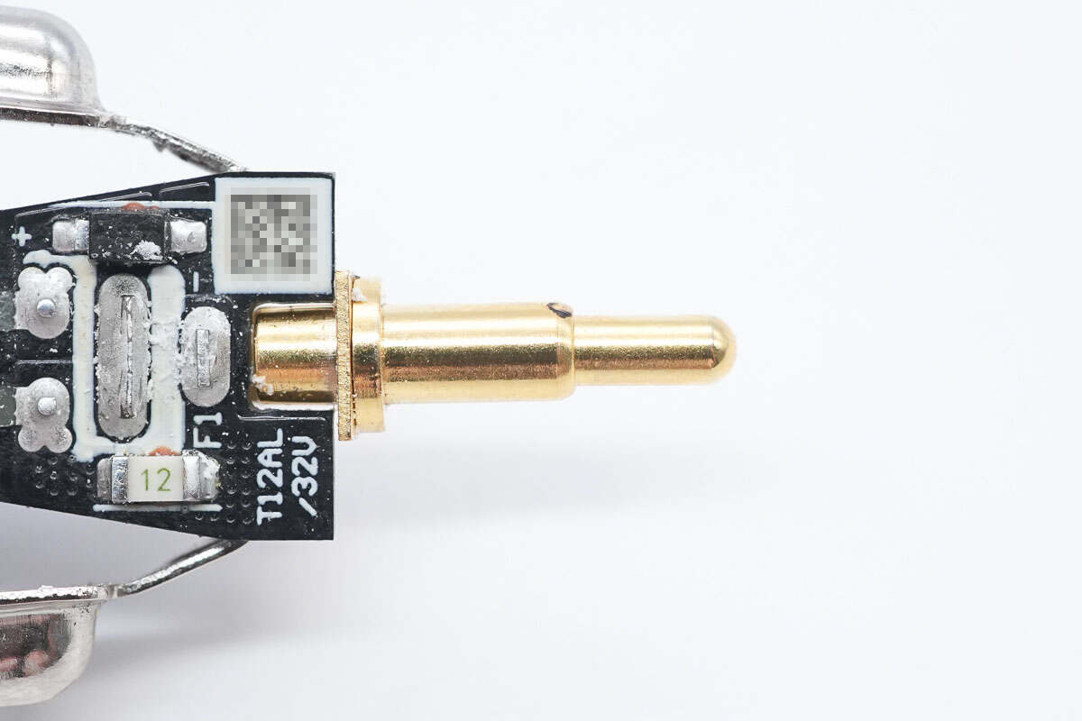
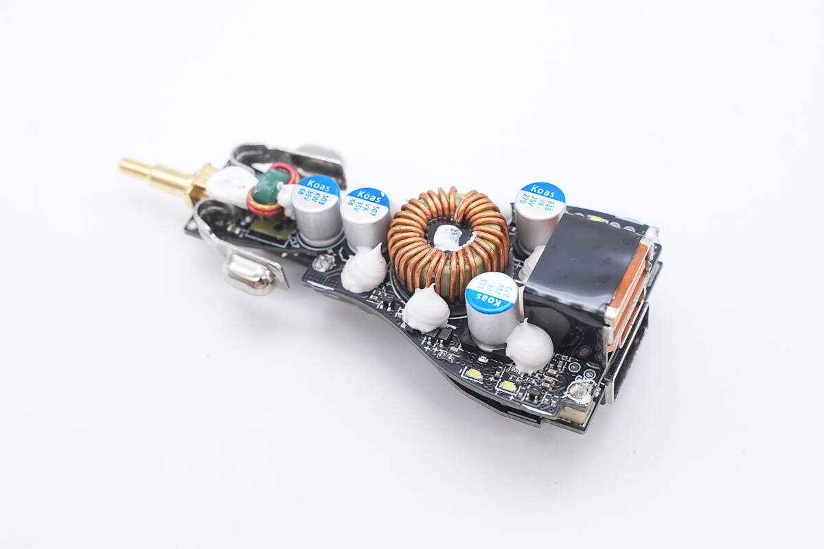
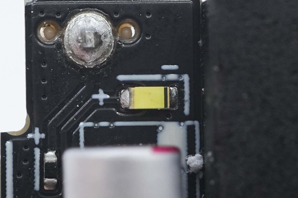
The positive conductive copper post is gold-plated.
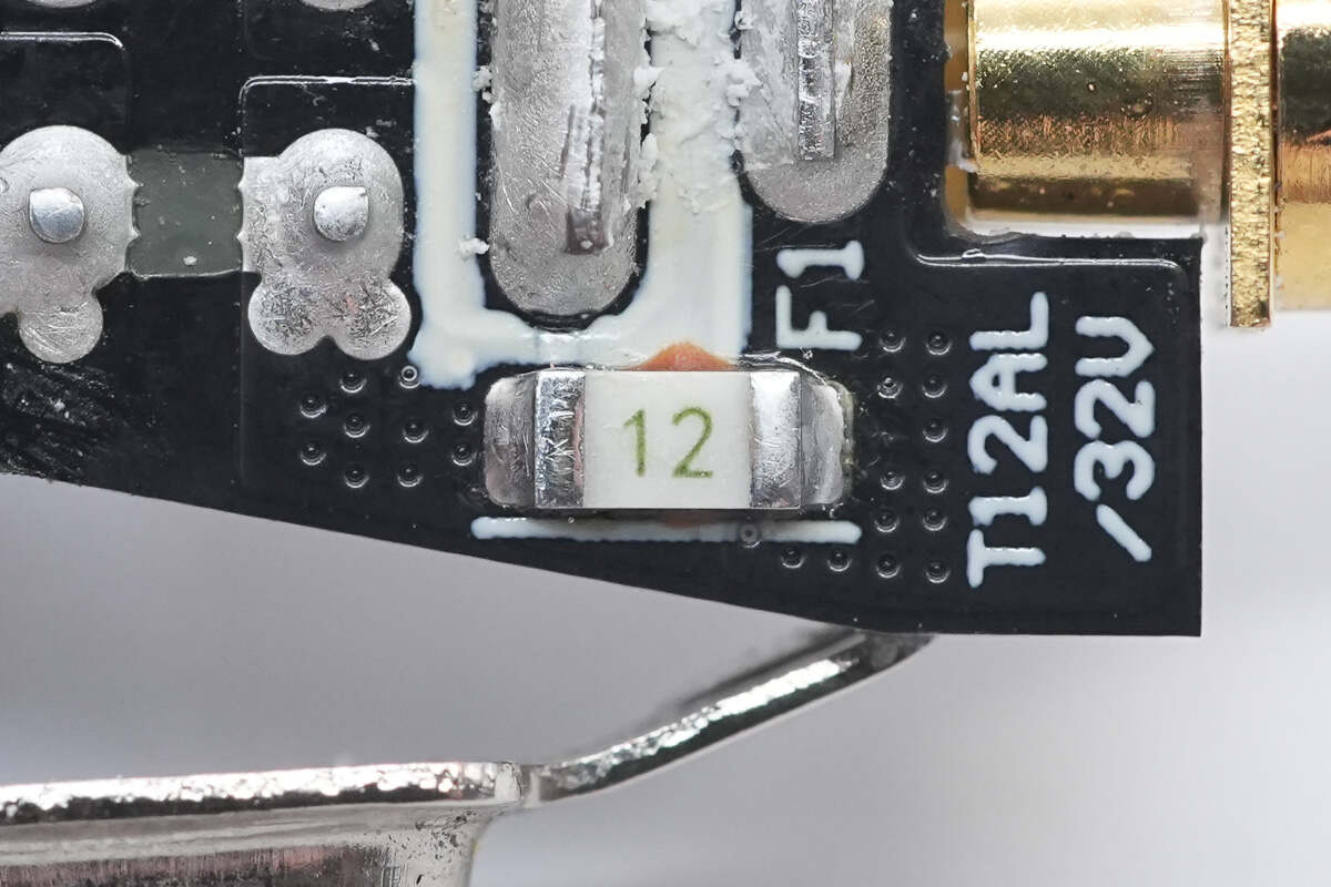
Close-up of the SMD fuse.
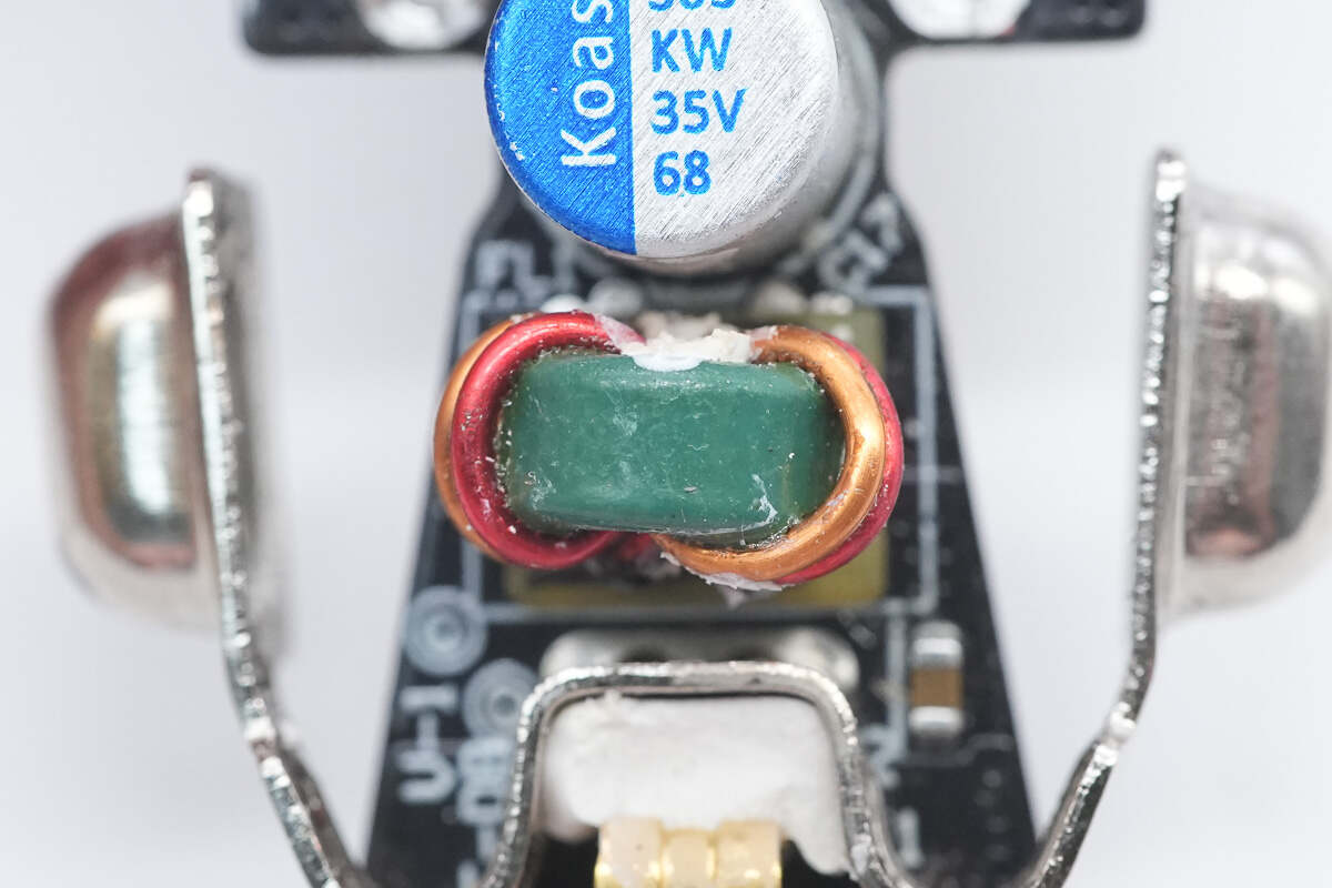
Close-up of the input filter inductor.
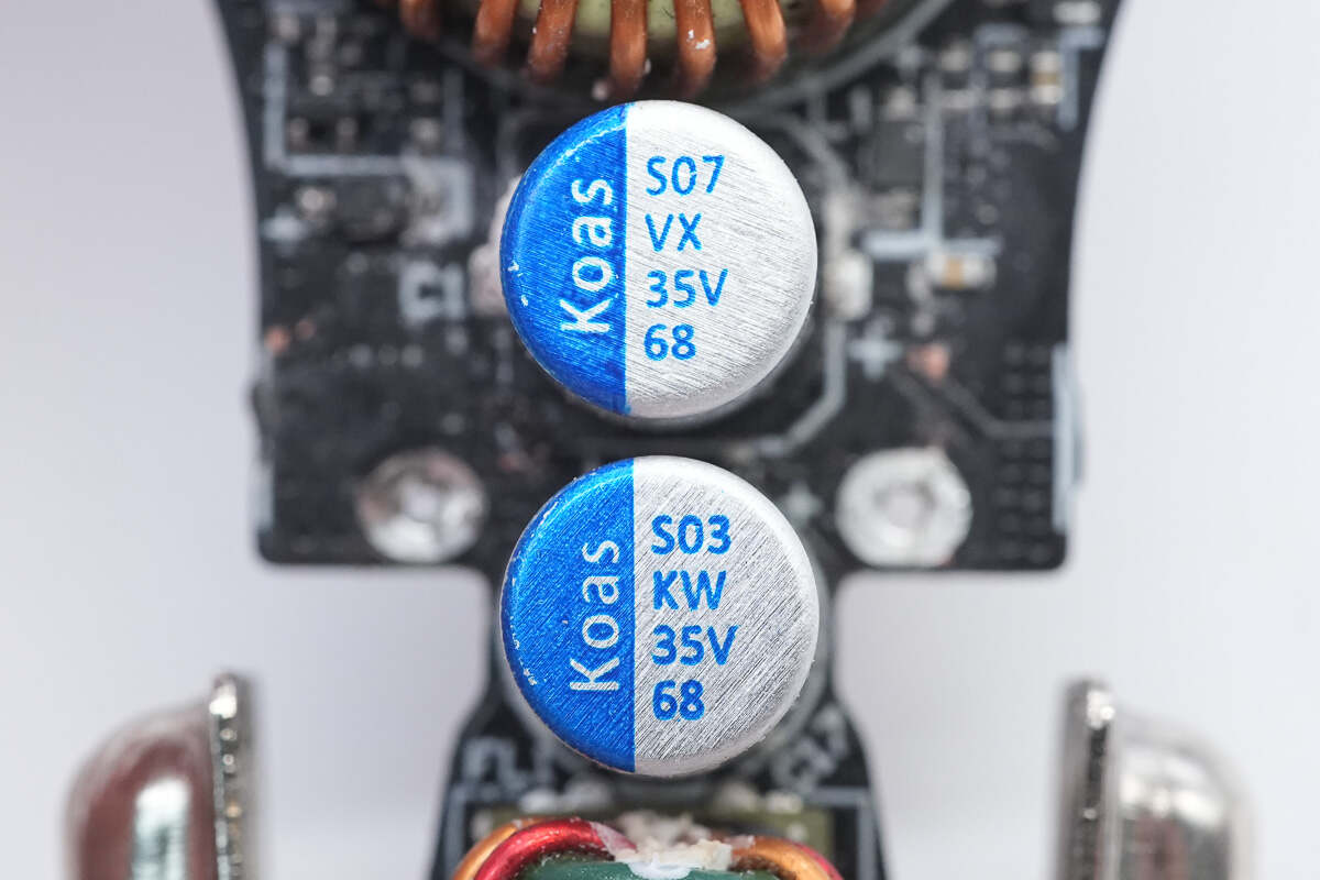
Both solid capacitors are rated at 35V 68μF.
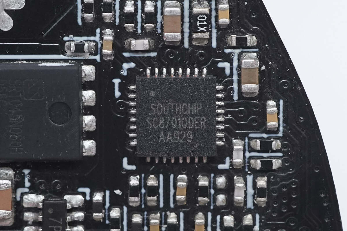
The synchronous buck-boost controller is from SouthChip, model SC8701. It is a 4-switch synchronous buck-boost controller capable of efficiently regulating the output voltage regardless of whether it is higher, lower, or equal to the input voltage. It supports a wide input and output voltage range, with input from 2.7V to 36V and output from 2V to 36V. The driver voltage is set to 10V to fully utilize external MOSFETs for maximum efficiency.
Here is the information about SouthChip SC8701.
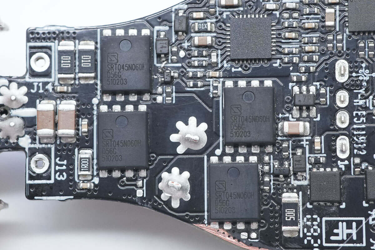
The four external synchronous buck-boost MOSFETs are model SRT045N060H. These are 45V-rated N-channel MOSFETs with an on-resistance of 5.1mΩ and come in a PDFN 5×6 package.
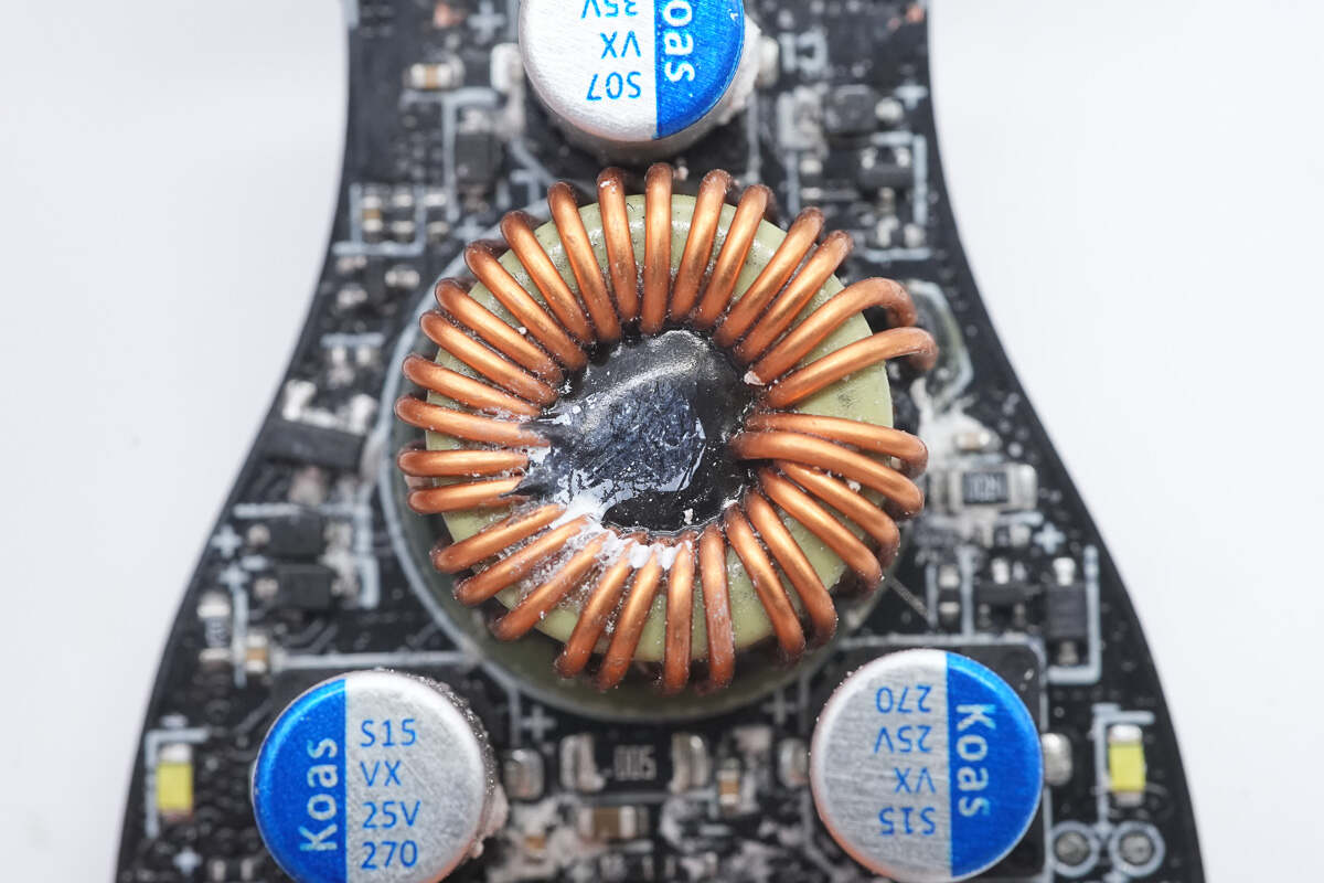
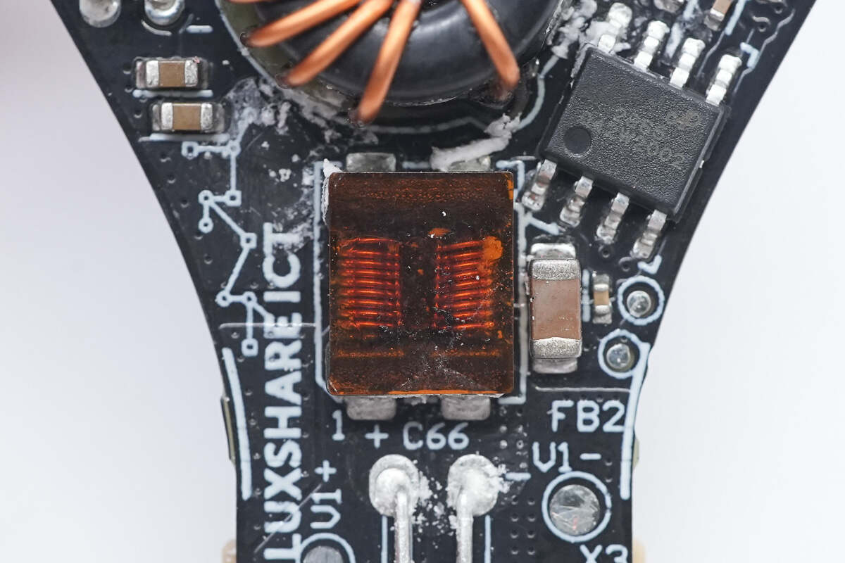
The buck-boost inductor is wounded with magnetic ring, and it's also insulated with bakelite.
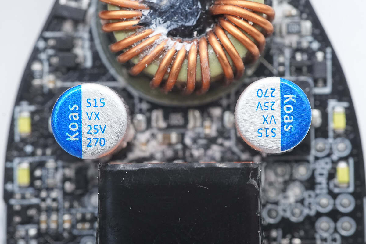
The two output filter capacitors are also from Koshin, each rated at 25V 270μF.
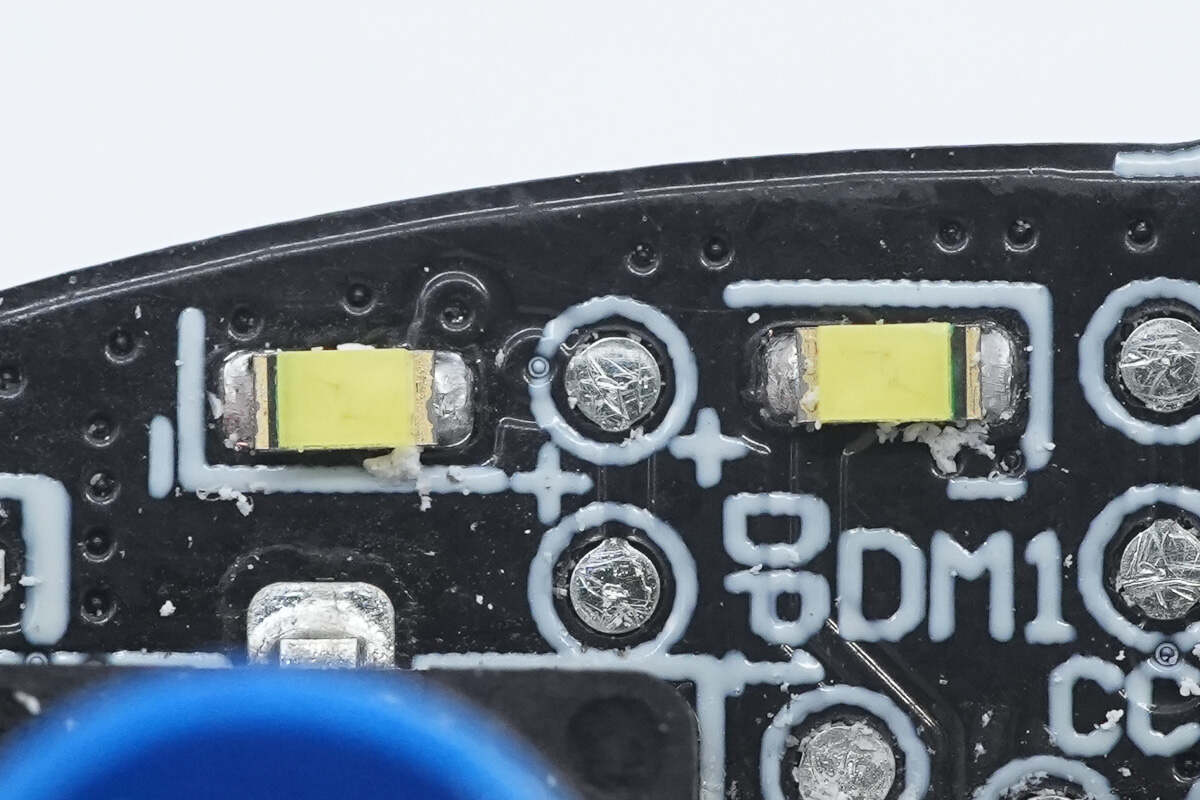
Close-up of the LED indicators located at the edge of the PCB.
Close-up of the LED indicators on the other edge of the PCB.
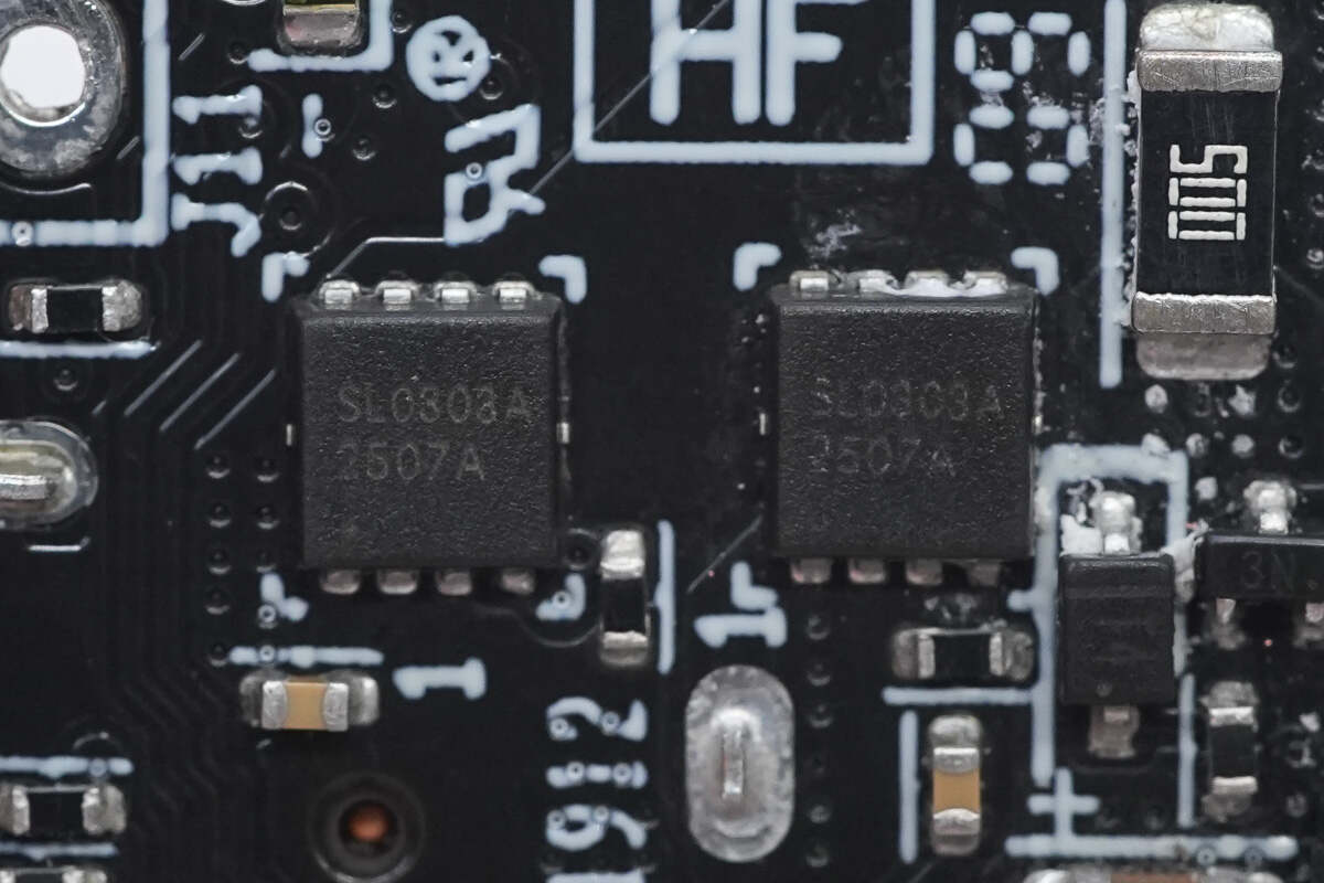
The two VBUS MOSFETs are from JieJie, model JMSL0303AU. These are 30V-rated N-channel MOSFETs with an on-resistance of 1.8mΩ, housed in a PDFN 3×3-8L package.
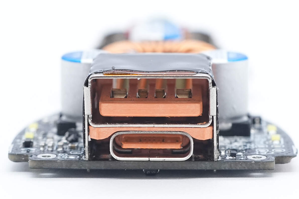
The combined port socket is reinforced and insulated with a steel sleeve and a Mylar sheet.
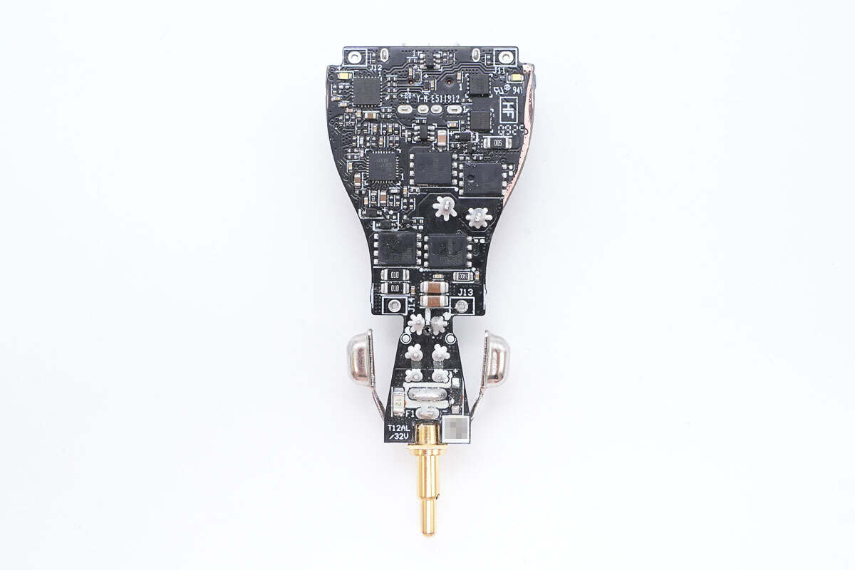
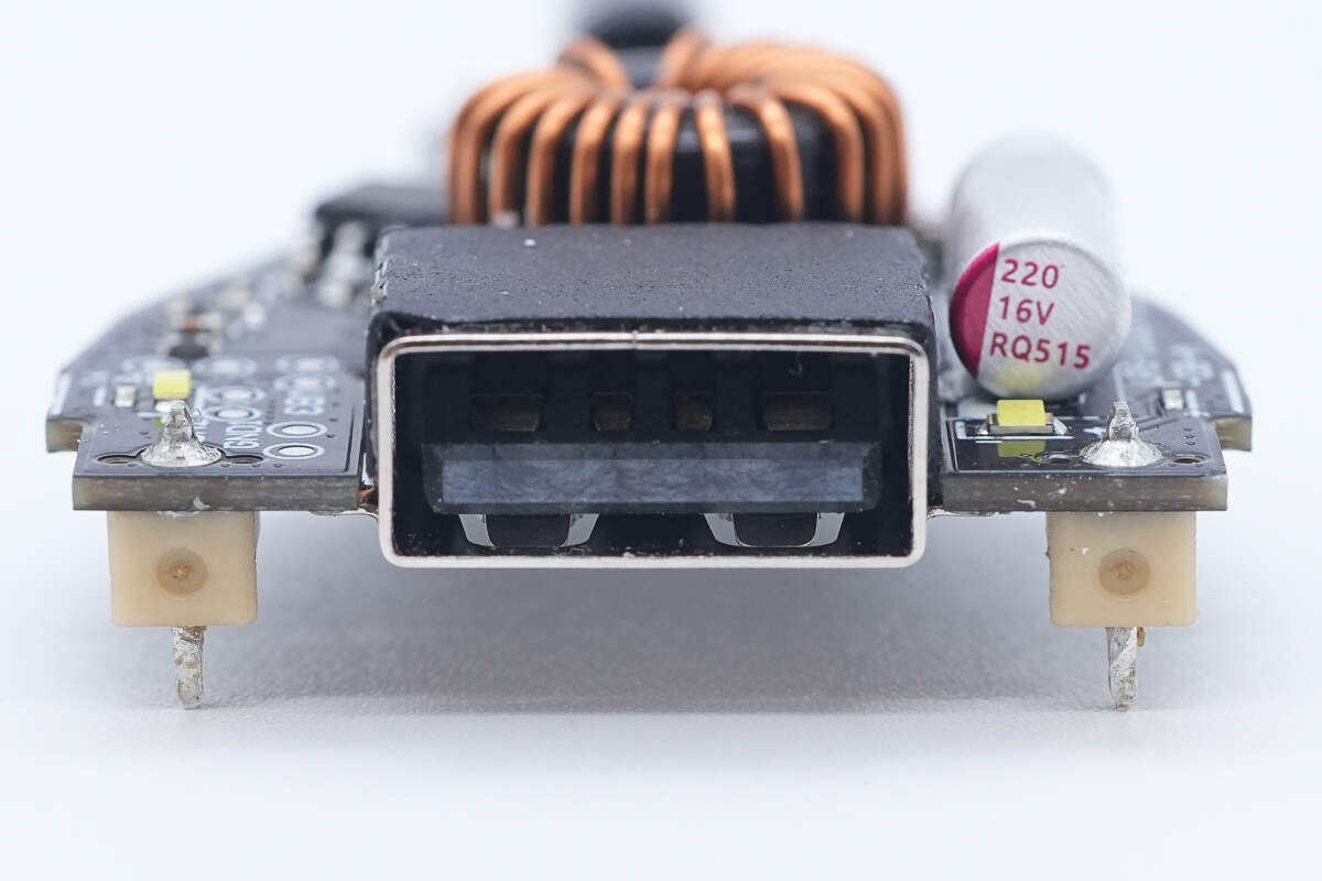
The front side of the other PCB features a filter inductor, capacitors, a synchronous buck converter, and a buck-boost inductor.
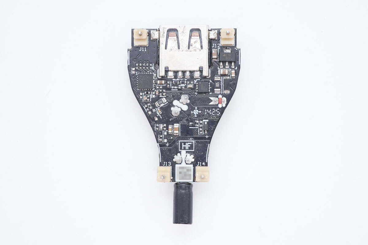
The other side has the protocol chip, output VBUS MOSFET, and the USB-A2 socket.
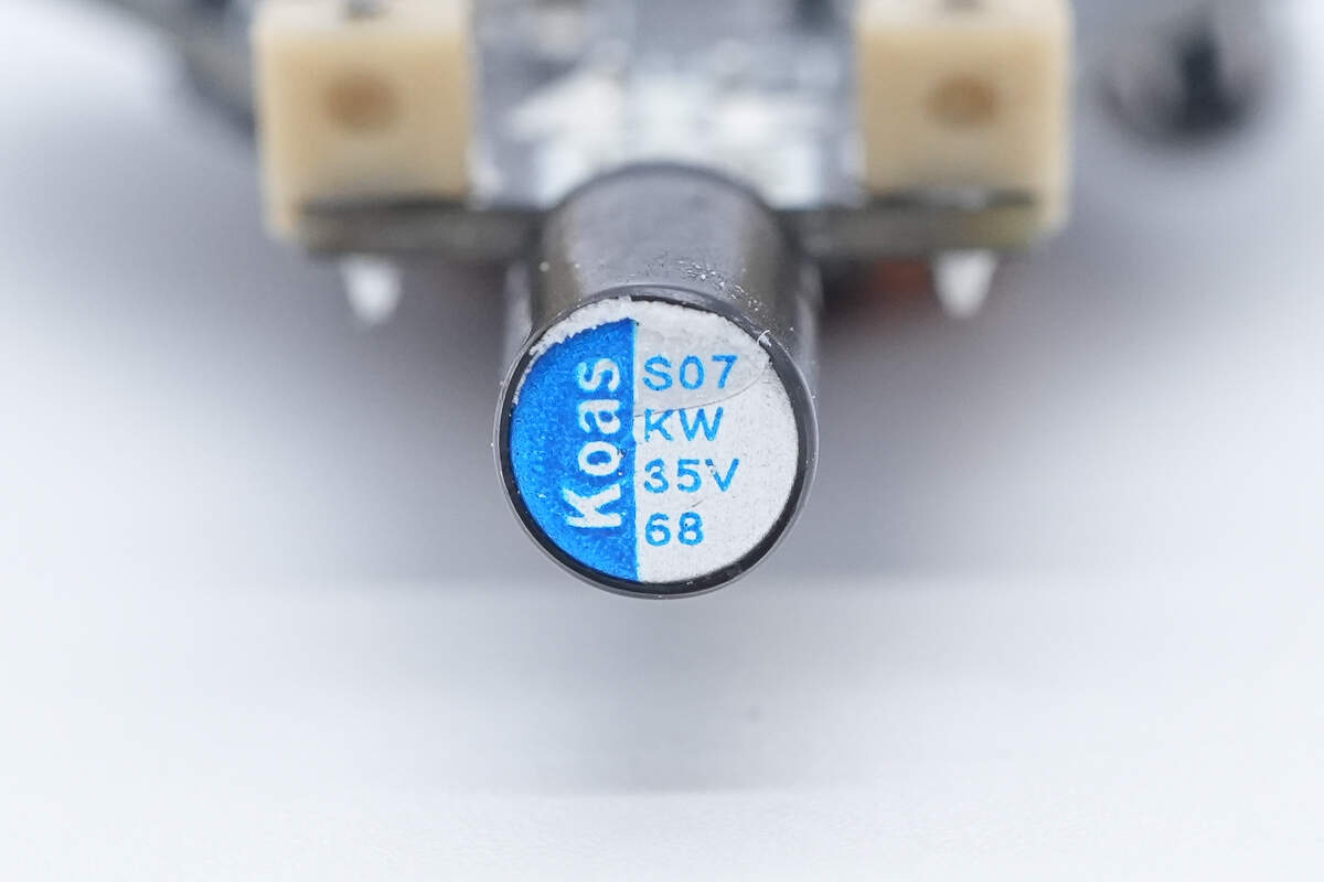
The solid capacitor for input filtering is also from Koshin, rated at 35V 68μF, and is insulated with heat-shrink tubing.
Close-up of the SMD filter inductor. The PCB is marked with "LUXSHARE ICT," indicating it is manufactured by Luxshare Precision.
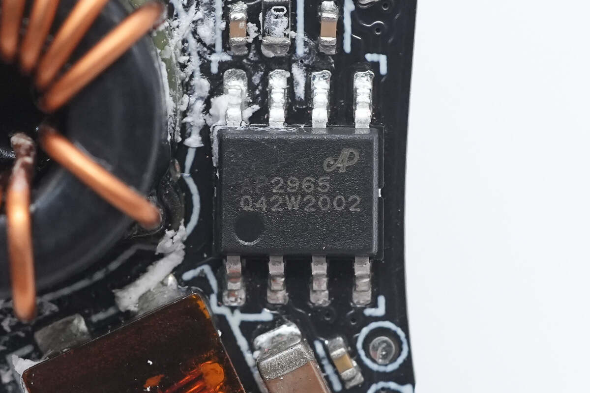
The synchronous buck converter is from Chipown, model AP2965. It supports a 40V input voltage and 4.2A output current. The device integrates internal MOSFETs, operates at a switching frequency of 130kHz, and features built-in soft-start and line-drop compensation. It also includes comprehensive protection functions.
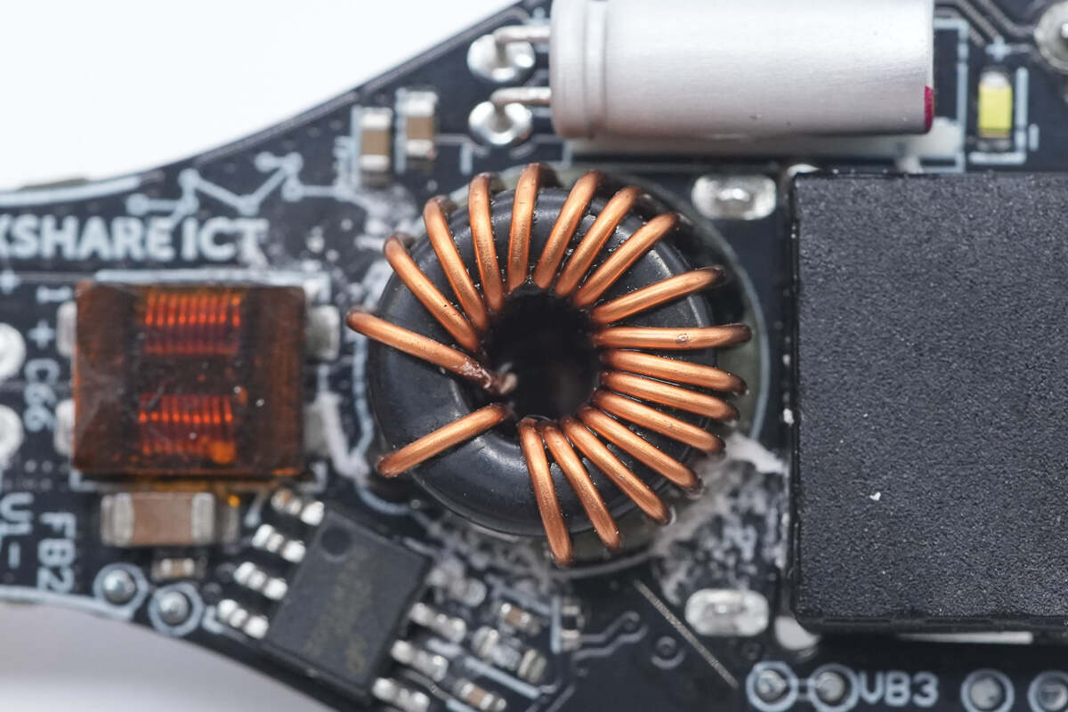
The magnetic buck inductor is insulated with bakelite.
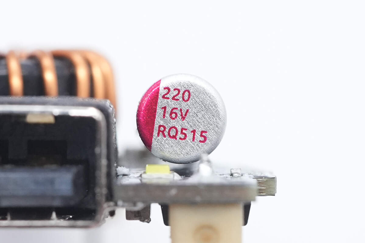
The buck output filter capacitor is rated at 16V 220μF.
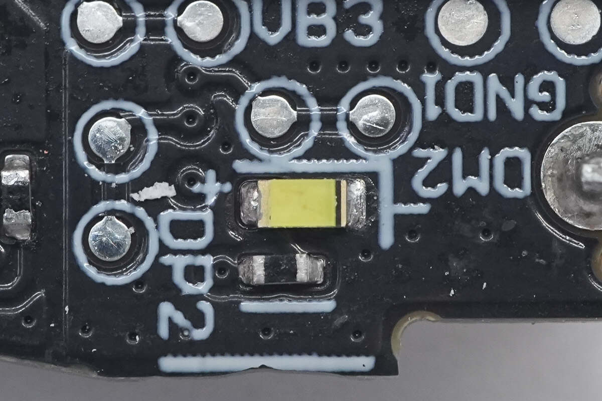
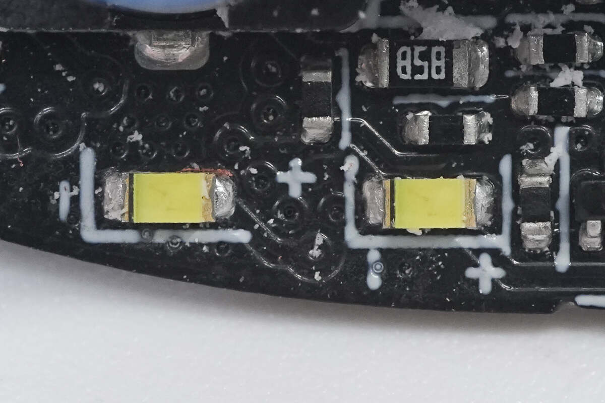
Close-up of the indicator LED on the PCB.
Close-up of the other indicator LED.
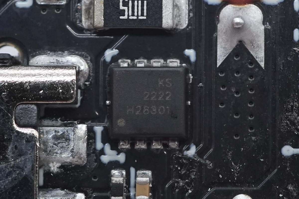
The output VBUS MOSFET is from Kwansemi, model KS2222. It is a 20V-rated N-channel MOSFET with an on-resistance of 5.9mΩ, packaged in a PDFN 3×3×3.
Close-up of the USB-A2 socket.
Well, those are all components of the HUAWEI 100W SuperCharge Car Charger.
Summary of ChargerLAB
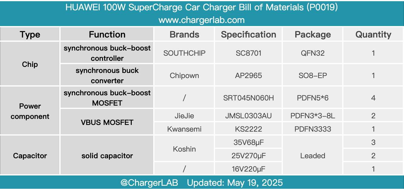
Here is the component list of the HUAWEI 100W SuperCharge Car Charger for your convenience.
It features a combined USB-A/USB-C port and a USB-A2 port, supporting a wide input voltage range of 12–24V. It maintains consistent output performance across different input voltages to ensure a reliable user experience. All ports support Huawei SuperCharge and UFCS protocols, with the USB-C port supporting 100W PD/PPS. Additionally, it supports output configurations of 100W+18W, 88W+22.5W, and 66W+30W.
After taking it apart, we found that it uses two separate circuits, regulated respectively by SouthChip SC8701 and Chipown AP2965 solutions. Capacitors, inductors, and other components on the PCB are reinforced with adhesive, and a thermal pad is placed between the two PCBs for heat dissipation. The USB sockets are insulated. In addition, it features comprehensive protection functions including input/output overvoltage/undervoltage, overcharge, output overcurrent, and short circuit protection, ensuring reliable quality.
Related Articles:
1. Teardown of Nintendo Switch 2 Official Charging Dock
2. Teardown of SHARGE Pixel 140 GaN Charger (S2)
3. Teardown of MEGMEET MR750‑20V 15 kW DC Charging Module